Hardware on hand: an STM32F407ZGT6 development board and an AD9959 DDS module.
By one evening, the high-frequency synchronization problem was basically solved. The next evening turned into a phase-control problem.
The basic idea is straightforward: instead of letting the DDS run from its onboard crystal, feed it with an external high-frequency reference. Once the DDS clock is tied directly to that external signal, its synthesized output must be derived from the same timing source, so frequency synchronization becomes possible in principle.
That only helps if the DDS side is already working normally, of course. The setup here was based on an AD9959 HAL driver found online; only ad9959.c and ad9959.h were reused, while the rest of the project was written separately.
There is one immediate constraint: the output signal is supposed to match the input signal frequency, but DDS output is digitally synthesized, so the DDS system clock has to be several times higher than the desired output. That means enabling the AD9959 internal PLL multiplier.
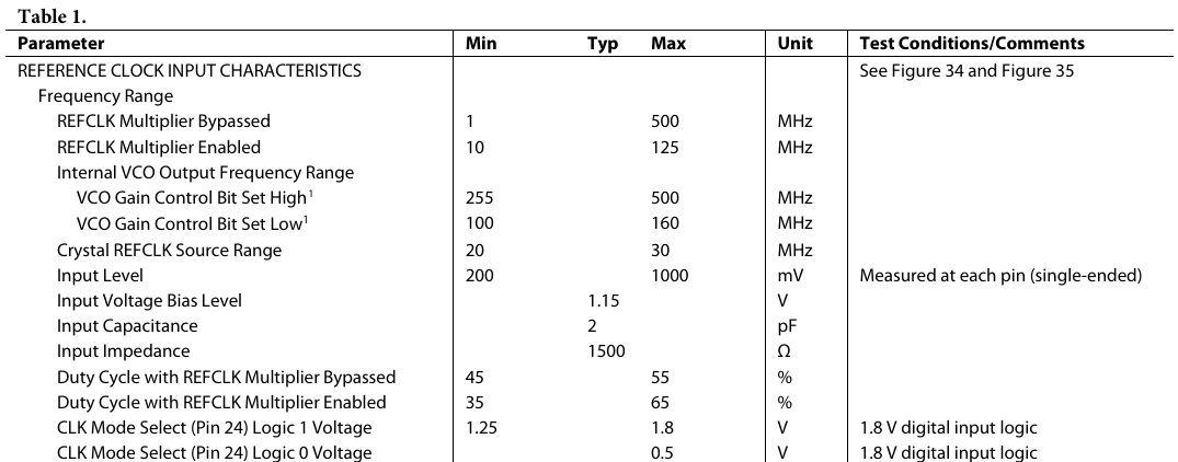
According to the AD9959 datasheet, under Frequency Range for REFCLK Multiplier Enabled, the allowed external reference clock range is 10–125 MHz when the multiplier is enabled.
A side note: the indentation in that table is misleading. Starting from the Internal VCO Output Frequency Range line, the formatting should really shift one level back. It is unfortunate to run into that as early as Table 1.
The more useful explanation actually appears later in the Reference Clock Modes section:
…As an alternative to clocking the part directly with a high frequency clock source, the system clock can be generated using the internal, PLL-based reference clock multiplier. …
Enabling the PLL allows multiplication of the reference clock frequency from 4× to 20×, in integer steps. …
…
Note that the output frequency of the PLL is restricted to a frequency range of 100 MHz to 500 MHz. However, there is a VCO gain control bit that must be used appropriately. The VCO gain control bit defines two ranges (low/high) of frequency output. The VCO gain control bit defaults to low (see Table 1 for details).
The key point is that the PLL can multiply the reference by any integer factor from 4 to 20.
Combining that with Table 1 gives the practical ranges:
- with the VCO gain control bit at its default low setting, the internal VCO output range is 100–160 MHz;
- with the bit set high, the range becomes 255–500 MHz.
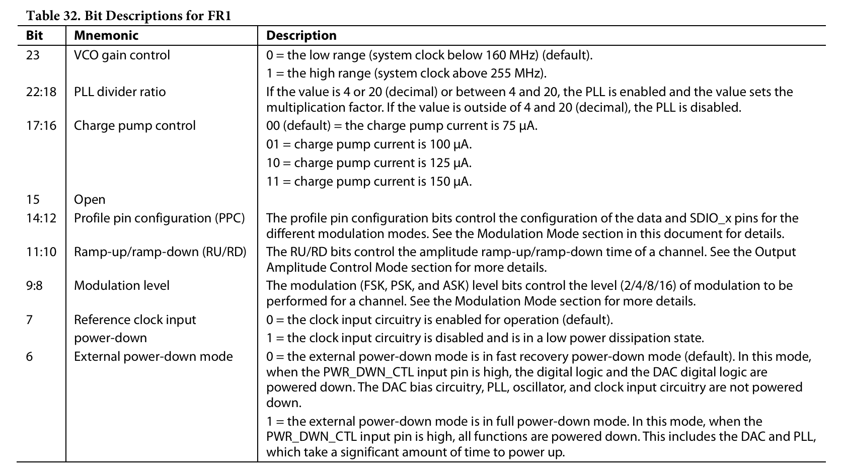
That VCO gain control bit is located in the FR1 register, together with the multiplier setting itself.
So both parameters are programmable. In the Init function of ad9959.c, the register was originally initialized like this:
1 2 3 4 5 6 7 8</th>
<th>uint8_t FR1_DATA[3] = {0xD3, 0x00, 0x00}; // 16 frequency doubling uint8_t CFR_DATA[3] = {0x00, 0x03, 0x00}; // default Value = 0x000302 _Init_AD9959_GPIO(); InitIO_9959(); InitReset(); WriteData_AD9959(FR1_ADD, 3, FR1_DATA); WriteData_AD9959(CFR_ADD, 3, CFR_DATA);</th>
</tr>
</thead>
<tbody>
<tr>
<td></td>
<td></td>
</tr>
</tbody>
</table>
A quick decode shows that 0xD30000 corresponds to 0b1101 0011 0000 0000 0000 0000 — or, in the datasheet grouping, roughly 0b1 10100 11 000…. That means:
VCO gain control = 1PLL divider ratio = 20(0b10100)
So the REFCLK is being multiplied by 20, and the result is expected to land above 255 MHz. The onboard crystal is marked 25 MHz, so after 20× multiplication the DDS system clock reaches 500 MHz, exactly the AD9959 upper limit.
Once the jumper is moved so the module uses an external input instead of the crystal, the allowed external frequency range becomes:
$$ f_{min}=\frac{255\text{MHz}}{20}=12.75\text{MHz} $$
$$ f_{max}=\frac{500\text{MHz}}{20}=25\text{MHz} $$
That 25 MHz upper limit may look surprisingly low compared with the 125 MHz maximum shown in Table 1. The reason is simply that the divider ratio here is set to 20. If the PLL divider ratio is reduced to its minimum of 4, then the valid external range becomes:
$$ f_{min}=\frac{255\text{MHz}}{4}=65.75\text{MHz} $$
$$ f_{max}=\frac{500\text{MHz}}{4}=125\text{MHz} $$
That aligns much better with the datasheet table. In practice, the multiplier has to be chosen according to the actual input frequency. If the input is even lower than 12.75 MHz, the VCO gain control bit can be cleared to 0, which lowers the VCO range from 255–500 MHz down to 100–160 MHz.
First attempt: frequency synchronization
The first test used the most direct possible method. Since the onboard crystal is 25 MHz, the jumper was switched from the crystal to the SMA input, then a 25 MHz signal from a signal generator was fed in. The DDS was programmed to output 25 MHz as well.
In theory, the synthesized 25 MHz should then be synchronized to the external 25 MHz reference.
But on the oscilloscope, the waveform kept drifting slowly. The movement was smooth and uniform, not jittering back and forth. That matters: it suggests the output really was derived from the external reference, but the configured output frequency was not exactly equal to the input frequency.
To see why, it helps to check what “setting the frequency” actually does in code.
This was the frequency-setting function in the original driver:
<table> <thead> <tr> <th>1 2 3 4 5 6 7 8 9 10 11 12 13 14 15 16 17 18 19</th>
<th>/** * @brief Writes the frequency value to the specified channel. * * @param Channel The channel number to write the frequency to.(0 to 3) * @param Freq The frequency value to be written.(1 to 500000000) */ void Write_Frequence(uint8_t Channel, uint32_t Freq) { if (Freq > 500000000 || Freq < 1) { Freq = 114514; AD9959_error(); } uint8_t CFTW0_DATA[4] = {0x00, 0x00, 0x00, 0x00}; Freq2Word(Freq, CFTW0_DATA); Channel_Select(Channel); WriteData_AD9959(CFTW0_ADD, 4, CFTW0_DATA); // CTW0 address 0x04.Output CH0 setting frequency }</th>
</tr>
</thead>
<tbody>
<tr>
<td></td>
<td></td>
</tr>
</tbody>
</table>
Most of that is routine: range checking, channel selection, register write. The interesting part is Freq2Word(), which converts a desired frequency into a tuning word:
1 2 3 4 5 6 7 8 9 10 11</th>
<th>void Freq2Word(double f, uint8_t *fWord) { // fWord 4 bytes uint32_t Temp; Temp = (uint32_t)f * 8.589934592; // The input frequency factor is divided into four bytes. 8.589934592=(2^32)/500000000 fWord[3] = (uint8_t)Temp; fWord[2] = (uint8_t)(Temp >> 8); fWord[1] = (uint8_t)(Temp >> 16); fWord[0] = (uint8_t)(Temp >> 24); }</th>
</tr>
</thead>
<tbody>
<tr>
<td></td>
<td></td>
</tr>
</tbody>
</table>
So the requested frequency is multiplied by a constant and then truncated into a 32-bit integer. The comment explains that constant:
$$ 8.589934592 = \frac{2^{32}}{500000000} $$
That 500 MHz is the DDS system clock — exactly what results from multiplying the 25 MHz crystal by 20. In other words, the DDS maps the frequency range from 0 to system clock into the 32-bit frequency tuning word range from 0 to $2^{32}$.
That makes the mismatch obvious. For a 25 MHz output:
$$ 25 \times 10^6 \times 8.589934592 = 214748364.8 $$
When that value is truncated to an integer, the 0.8 is lost.
It might be tempting to blame floating-point arithmetic and replace the multiplication with integer math. But that does not solve it:
$$ 2^{32}\times\frac{25M}{500M}=214748364.8 $$
The same fractional result appears. The issue is not floating-point error at all. The real problem is that $2^{32}$ is not divisible by 20, so with a PLL multiplier of 20, some frequencies simply cannot map exactly to an integer tuning word.
Choosing a multiplier that fits the tuning word math
The fix is to use a PLL divider ratio that divides cleanly into $2^{32}$. Among the available multipliers, that leaves 4, 8, and 16. Here, the ratio was changed to 16. Then, in Freq2Word(), the old coefficient was multiplied by 2.5 to account for the reduced system clock.
To set the PLL divider ratio to 16, the FR1 register becomes 0xC30000, corresponding to 0b1 10000 11 0000….
The initialization changed to:
<table> <thead> <tr> <th>1 2 3 4 5 6 7 8</th>
<th>uint8_t FR1_DATA[3] = {0xC3, 0x00, 0x00}; // 16 frequency doubling uint8_t CFR_DATA[3] = {0x00, 0x03, 0x00}; // default Value = 0x000302 _Init_AD9959_GPIO(); InitIO_9959(); InitReset(); WriteData_AD9959(FR1_ADD, 3, FR1_DATA); WriteData_AD9959(CFR_ADD, 3, CFR_DATA);</th>
</tr>
</thead>
<tbody>
<tr>
<td></td>
<td></td>
</tr>
</tbody>
</table>
And the frequency conversion function became:
<table> <thead> <tr> <th>1 2 3 4 5 6 7 8 9 10</th>
<th>void Freq2Word(double f, uint8_t *fWord) { // fWord 4 bytes uint32_t Temp; Temp = (uint32_t)f * 8.589934592 * 2.5; // The input frequency factor is divided into four bytes. 8.589934592=(2^32)/500000000 fWord[3] = (uint8_t)Temp; fWord[2] = (uint8_t)(Temp >> 8); fWord[1] = (uint8_t)(Temp >> 16); fWord[0] = (uint8_t)(Temp >> 24); }</th>
</tr>
</thead>
<tbody>
<tr>
<td></td>
<td></td>
</tr>
</tbody>
</table>
After that, slowly adjusting the signal generator frequency made the DDS output track along with it, and the two waveforms stayed relatively stationary on the oscilloscope. Frequency synchronization was now working well enough.
That looked like a win.
Then the phase problem showed up
The next day, another round of testing ruined the celebration a bit.
Although frequency sync was working, the phase difference between input and output was not fixed. After every restart, the system locked with a different phase offset. In practice, the output would repeatedly land near one of four values: -98°, -8°, +82°, or +172°.
So the PLL had solved one problem and introduced another: the DDS could lock to the reference, but the startup phase was not deterministic.
That changed the goal from “make the frequency match” to “make the phase match too.”
The AD9959 already supports programmable output phase from 0° to 359° in 1° steps. So if the MCU can measure the current phase difference, correcting it should be straightforward.
The obvious approach is to insert a phase detector between the reference clock and the DDS output. Its output is typically a DC voltage that corresponds to phase difference. Feed that voltage into an ADC, then adjust the DDS phase until the detector indicates alignment.
A phase detector was borrowed and tested first using a signal generator and oscilloscope. The observed behavior was simple enough: the smaller the phase difference, the higher the detector output voltage. The usable range was roughly 40 mV to 1.9 V, which is easy to sample with the ADC.
There was one warning worth keeping in mind: the detector input should not exceed 0 dBm, which works out to roughly 300 mV peak. Meanwhile, Table 1 of the AD9959 gives an input range of 200 mV to 1000 mV, so the chosen levels were still usable.
Measurement setup
The wiring looked like this:
- the signal generator provided the reference signal;
- that same reference was sent to oscilloscope channel 1, the DDS
REFCLK, and one input of the phase detector; - the DDS output went to oscilloscope channel 2 and the other input of the phase detector;
- the phase detector output was connected to the MCU ADC.
For the first demo, the control logic was deliberately brute-force: sweep through all 360 possible phase settings, read the ADC each time, and keep the phase that produces the highest voltage.
Testing showed a consistent extra 20° phase offset in the output. Interestingly, that offset did not change after MCU resets. The maximum detected ADC level was indeed around 1.9 V. At that point, this stopped being a theoretical purity contest and became an engineering task, so an extra 20° correction was simply added manually.
The code was then improved a bit. Scanning all 360 degrees was unnecessarily slow. Since the ADC value already indicates how far away the phase is from alignment, the step size can be made larger when the voltage is low, allowing the search to jump quickly and then refine near the peak. A loop count limit was added as well.
The final control loop looked like this:
<table> <thead> <tr> <th>1 2 3 4 5 6 7 8 9 10 11 12 13 14 15 16 17 18 19 20 21</th>
<th>uint16_t max=0, temp=0, i=0, cnt=0; while (max<2500 && cnt<50) { Write_Phase(1, i); AD9959_IO_Update(); delay_ms(10); temp=Get_Adc_Average(ADC_CHANNEL_0, 20); if (max<temp) { max=temp; phase0=i; } i+=60*(2500-temp)/2500; i%=360; cnt+=1; } //phase0+=26; phase0+=20; phase0%=360; Write_Phase(1, phase0); AD9959_IO_Update(); LCD_ShowString(0, lcddev.height-40, 320, 32, 32, (u8*)"synchronized!");</th>
</tr>
</thead>
<tbody>
<tr>
<td></td>
<td></td>
</tr>
</tbody>
</table>
With that in place, the final result was quite decent: the DDS could be synchronized to an external high-frequency reference, and the phase could be adjusted into place after startup rather than being left to PLL luck.
There was supposed to be a test video too, but that part never made it online.